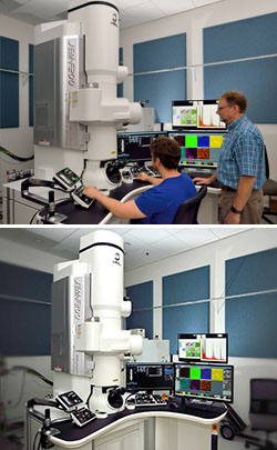
Skip to:

MRFN Member Login
Program Application

Electron Microscopy Facility

Location: Singh Center for Nanotechnology
Supervisor/Coordinator: Douglas Yates
Contact: Douglas Yates
Phone: 215-898-2013
Email: dmyates@seas.upenn.edu
Oversight Committee Chair: Christopher B. Murray, MSE
 

The Nanoscale Characterization Facility maintains a full-service electron microscopy facility equipped with a wide range of state-of-the-art instrumentation for materials analysis. Structural, chemical and microstructural characterization of polymers, ceramics, composites, metals and alloys, electronic materials and devices, thin films, and coatings are conducted using scanning electron microscopes, focused ion beam electron microscopes, transmission electron microscopes, and scanning transmission electron microscopes. A wide range of specimen preparation equipment is used including cryo-ultramicrotomy, cryo-plunge, jet electrolytic polishing, mechanical dimpling, tripod polishing, vacuum evaporation, sputter-coating and replication. In-house hardware and software are available for a wide range of image and spectrum processing tasks and for the calculation/simulation of electron-beam specimen interactions and microscope performance. Facility staff provide complete user training and assistance with research projects involving our instruments. The staff are also available for demand service in situations where training is not desired.

  • Microscopy Instruments include:
    • Field-Emission Scanning Electron Microscope – JEOL 7500F HRSEM
    • Environmental Scanning Electron Microscope – FEI 600 Quanta FEG SEM
    • Focused Ion Beam – FEI Strata DB235 FIB
    • Aberration Corrected Scanning/Transmission Electron Microscope – JEOL NEOARM TEM/STEM
    • JOEL F200 TEM/STEM
  • TEM/STEM/EFTEM

Instruments

  1. F200 scanning / transmission electron microscope

    The JEOL F200 is a 200kV scanning / transmission electron microscope with a cold field emission source, two large area energy dispersive x-ray spectrometers, and Gatan OneView IS camera for in situ/operando imaging at 30 frames per second. It incorporates STEMx capability.

  2. FEI 600 Quanta FEG ESEM

    The Quanta 600 FEG Mark II scanning electron microscope (SEM) is equipped with a unique array of accessories to enable the combination of high-resolution imaging and nanoscale manipulation allowing for powerful in situ experiments involving controlled stimuli and correlated response.

  3. FEI Strata DB235 Focused Ion Beam

    The FEI Strata DB235 Focused Ion Beam bridges the gap between nanocharacterization and nanomachining by combining a high resolution field-emission scanning electron microscope with a focused ion beam. Uniting these techniques in a single instrument allows users to seamlessly switch from secondary electron imaging to precision ion milling and ion-beam assisted material depostion and selective etching. Four gas injection systems will allow for platinum deposition and selective etching of carbon, metals, and oxides.

  4. JEOL 2010 TEM

    The JEOL 2010 TEM is available for both conventional and high resolution TEM imaging. It is equipped with single tilt, double-tilt, heating and cooling sample holders for a wide range of imaging experiments. The analytical objective lens pole piece on this microscope allows for sample tilting up to 45 degrees, yet maintains a point-to-point resolution of 0.25 nm. In addition to the conventional plate camera, this instrument is equipped with a Gatan Peltier cooled CCD imaging system for high quality digital imaging.

  5. JEOL 2010F FEG HRTEM

    The JEOL 2010F TEM/STEM is a state-of-the-art field emission transmission electron microscope with capabilities ranging from nanobeam and convergent beam diffraction to high resolution phase contrast, analytical and energy filtered imaging. The 2010F has been optimized for analytical microscopy with a large solid angle for high X-ray throughput, scanning, scanning-transmission, and backscattered electron detectors and a Gatan image filter for energy filtered imaging and electron energy loss spectroscopy.

  6. JEOL 7500F HRSEM

    The JEOL 7500F scanning electron microscope (SEM) is our dedicated conventional and high-resolution imaging microscope. It is equipped with a range of detectors and imaging modes that allow for the study of a wide range of solid materials. Secondary and backscattered electron detectors allow for imaging of sample surfaces, whereas a scanning-transmission electron detector shows the internal structure of materials.

  7. NEOARM Aberration-corrected scanning / transmission electron microscope

    The JEOL NEOARM is a scanning / transmission electron microscope, equipped with a spherical aberration corrector for the probe-forming optics. This corrector has improved stability and optimizes 5th order aberrations, leading to <0.7Å imaging at 200kV, and <1.6Å at 30kV. The instrument is a high-brightness cold field emission instrument. It is equipped with two large area energy dispersive x-ray spectrometers that permit rapid atomic-resolution EDS mapping.